Can China build its own ASML?
Beijing wants 100% domestic chip equipment, but lithography remains an uphill battle

Can China build its own ASML?
Beijing wants 100% domestic chip equipment, but lithography remains an uphill battle
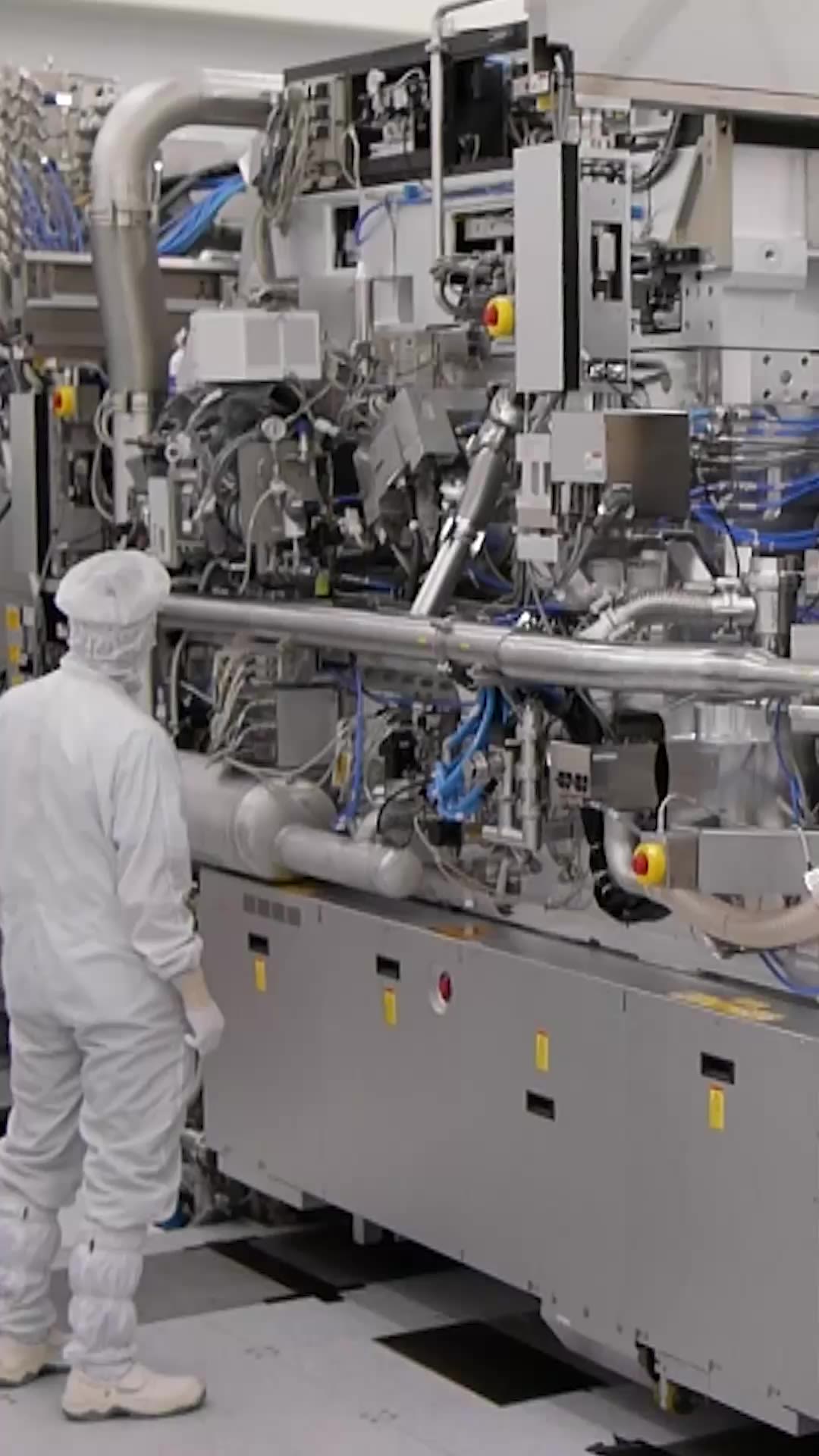

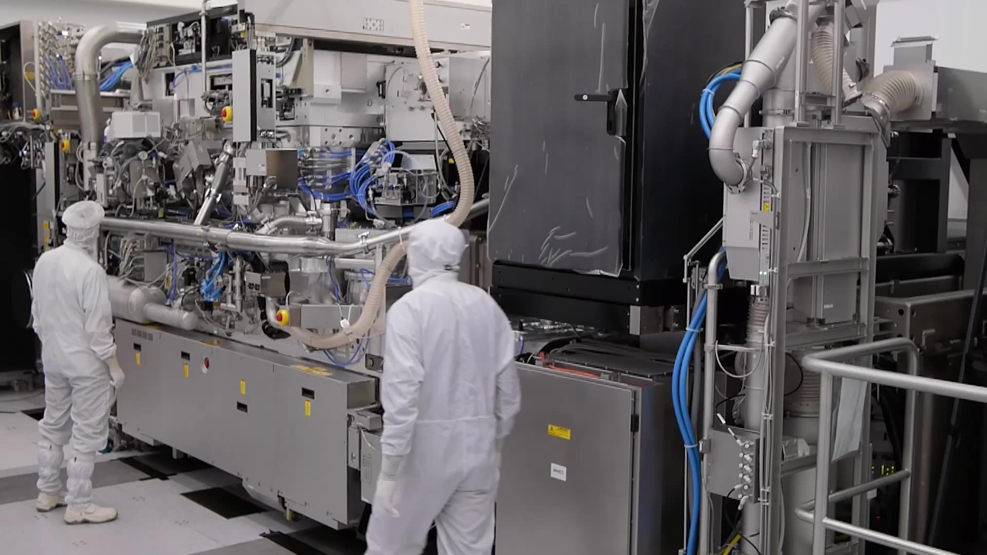
In southeastern Beijing, engineers at Semiconductor Manufacturing International Corp., China's top chipmaker, are working around the clock to expand the output of 14-nanometer and even 7-nm chips, just a few generations behind the world's leading chipmakers. Being able to make such advanced chips at all is a major breakthrough for a company that has been laboring under a U.S. blacklisting for five years.
But SMIC's mission goes beyond just making the chips. It wants to produce them entirely with Chinese equipment.
That goal -- a fully domestic chip equipment supply chain -- is laid out explicitly in the city’s 14th Five-Year Plan, an economic roadmap for the capital, and the nation’s chipmakers are pushing hard to make it a reality, even if it means sacrificing production quality and efficiency in the short term, sources tell Nikkei Asia.
SMIC and its peers, including local leading memory makers CXMT and YMTC, have achieved striking progress on several fronts, replacing foreign tools used for etching, measurements, deposition, chemical polishing and more with domestic alternatives, according to multiple interviews with industry executives by Nikkei Asia.
But one daunting hurdle remains: lithography.
The process of projecting and printing chip developers' designs onto a wafer is vital to the ultimate performance of the chip. But lithography machines are so complex and expensive that only three companies in the world -- ASML of the Netherlands and Japan's Canon and Nikon -- are capable of producing them. Last year, lithography accounted for nearly 25% of global spending on chipmaking equipment, according to industry group SEMI.

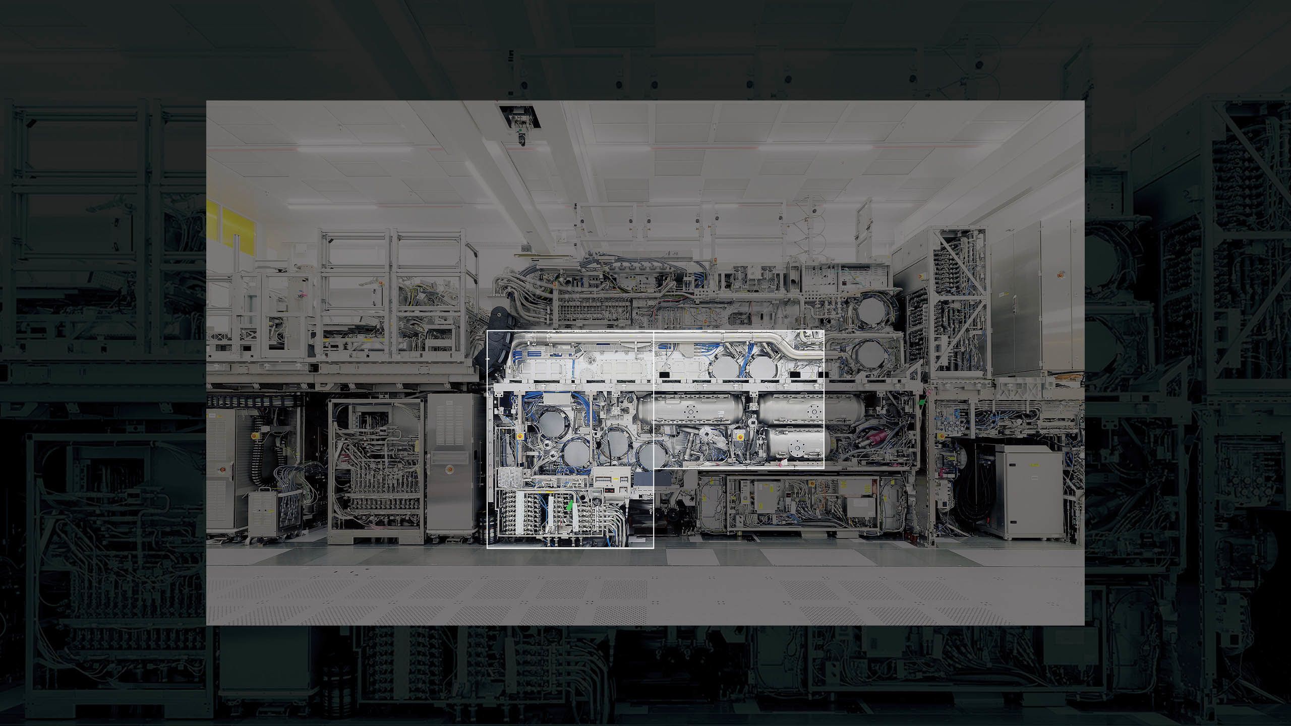
Top Chinese chipmaker SMIC is expanding plants in Beijing to make 7-nm and 14-nm chips, the most advanced in the nation.
Top Chinese chipmaker SMIC is expanding plants in Beijing to make 7-nm and 14-nm chips, the most advanced in the nation.
For China, this remains a painful gap in its push for tech self-sufficiency.
"Local lithography tools are still a blank spot and [China is] nowhere close to being self-sufficient," said one supply chain executive who counts major Chinese chipmakers as clients. "Most production lines are still using ASML or Nikon machines, even if those are their older models."
ASML is the largest global chip tool maker by market capitalization, as well as the leader in immersion deep ultraviolet (DUV) technology, used to make chips for everything from smartphones to cars to defense equipment. The Dutch company is also the exclusive maker of extreme ultraviolet (EUV) lithography tools, which chip titans like TSMC, Samsung and Intel use to make the world's most advanced processors and memory chips.
At its headquarters in Veldhoven, engineers are already busy putting the final touches on an even more advanced machine, one that ASML hopes will support cutting-edge chip production through the early 2030s.
The high-NA EUV machine, as it is called, is now being shipped to TSMC and Intel for field trials, and the company expects broader industry adoption to follow. At $350 million apiece, the machine is the most expensive chipmaking tool ever built.
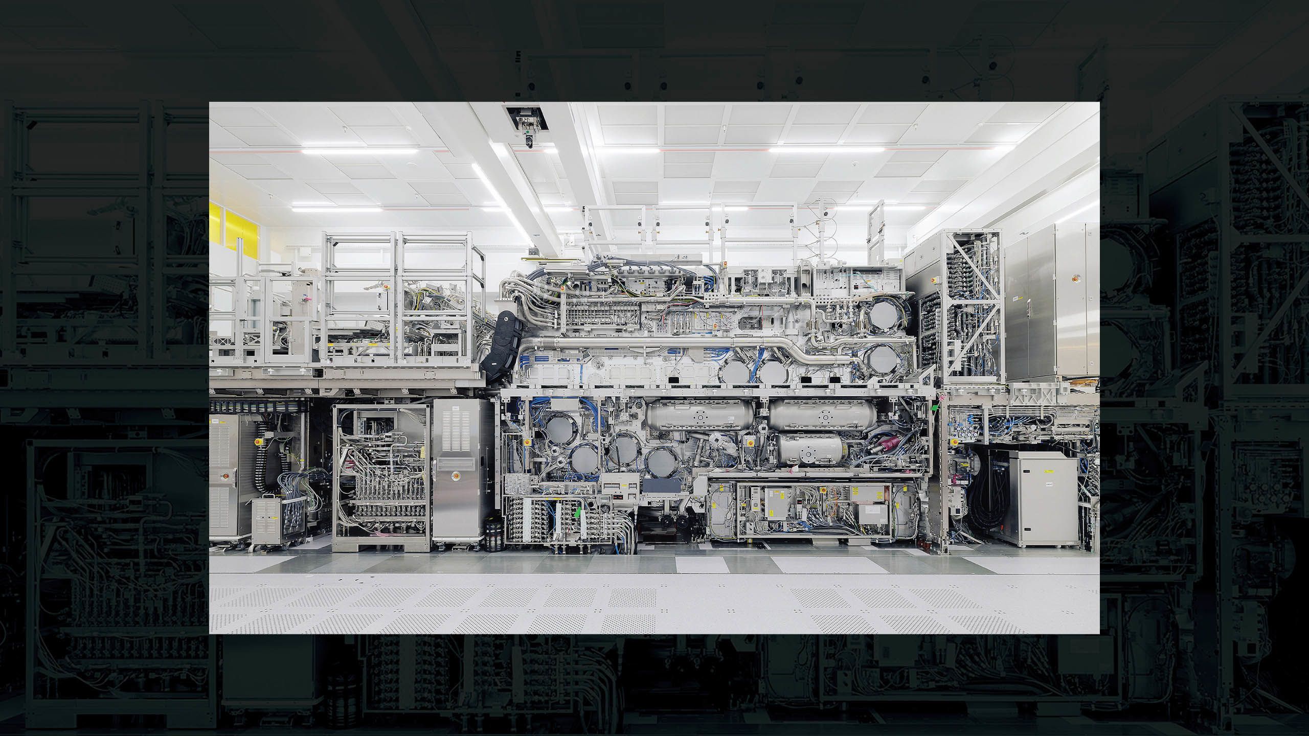
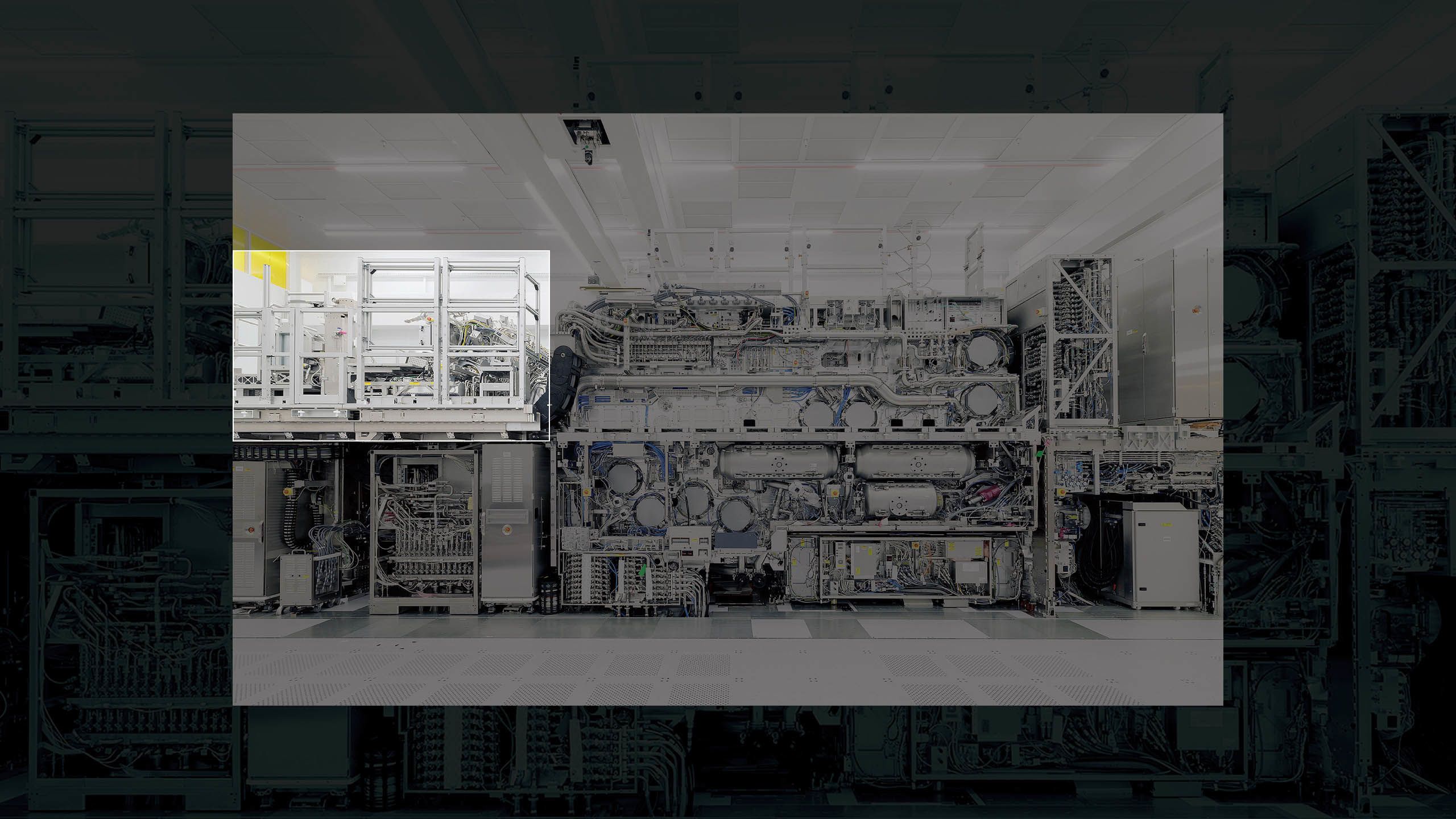
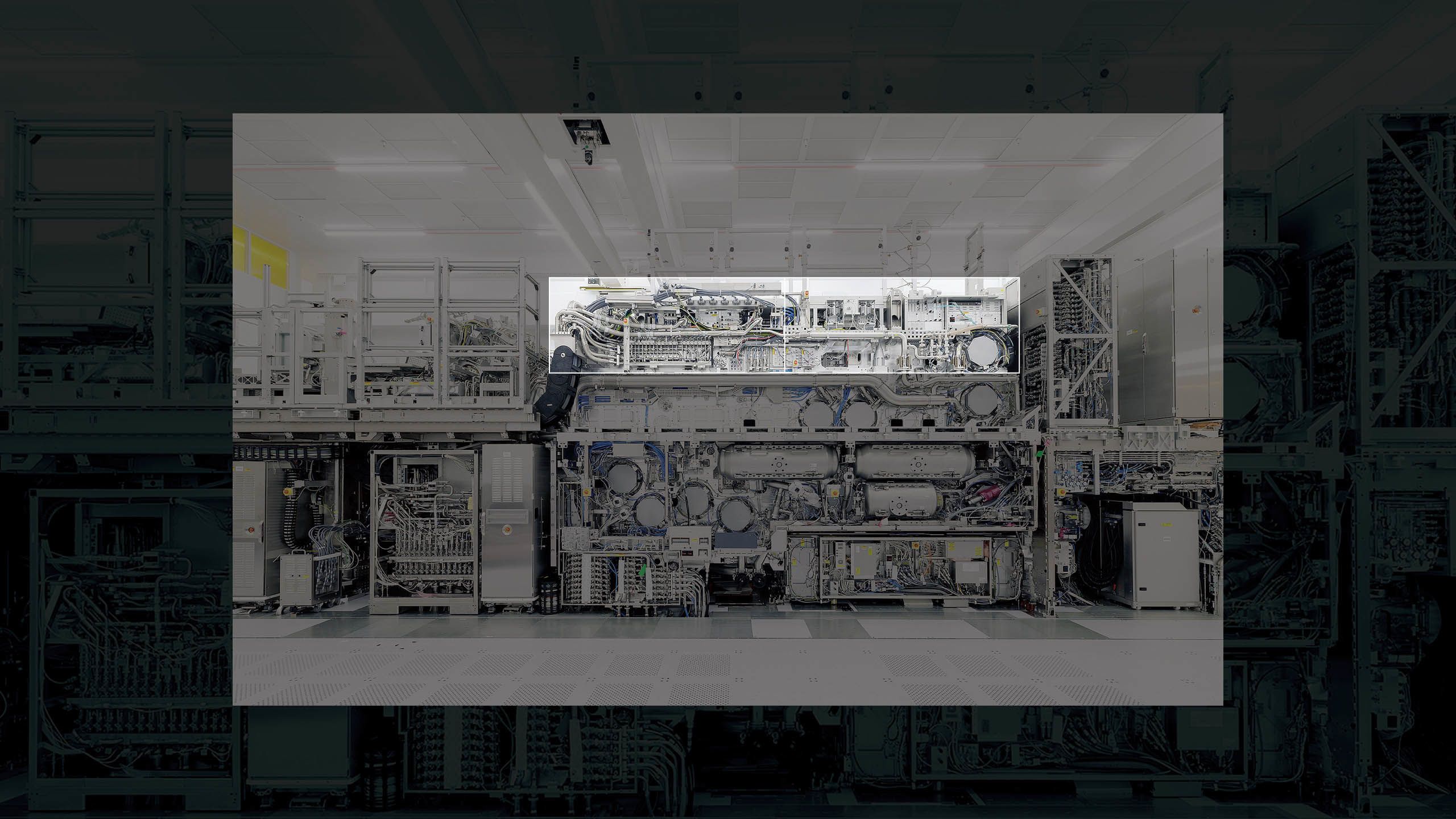
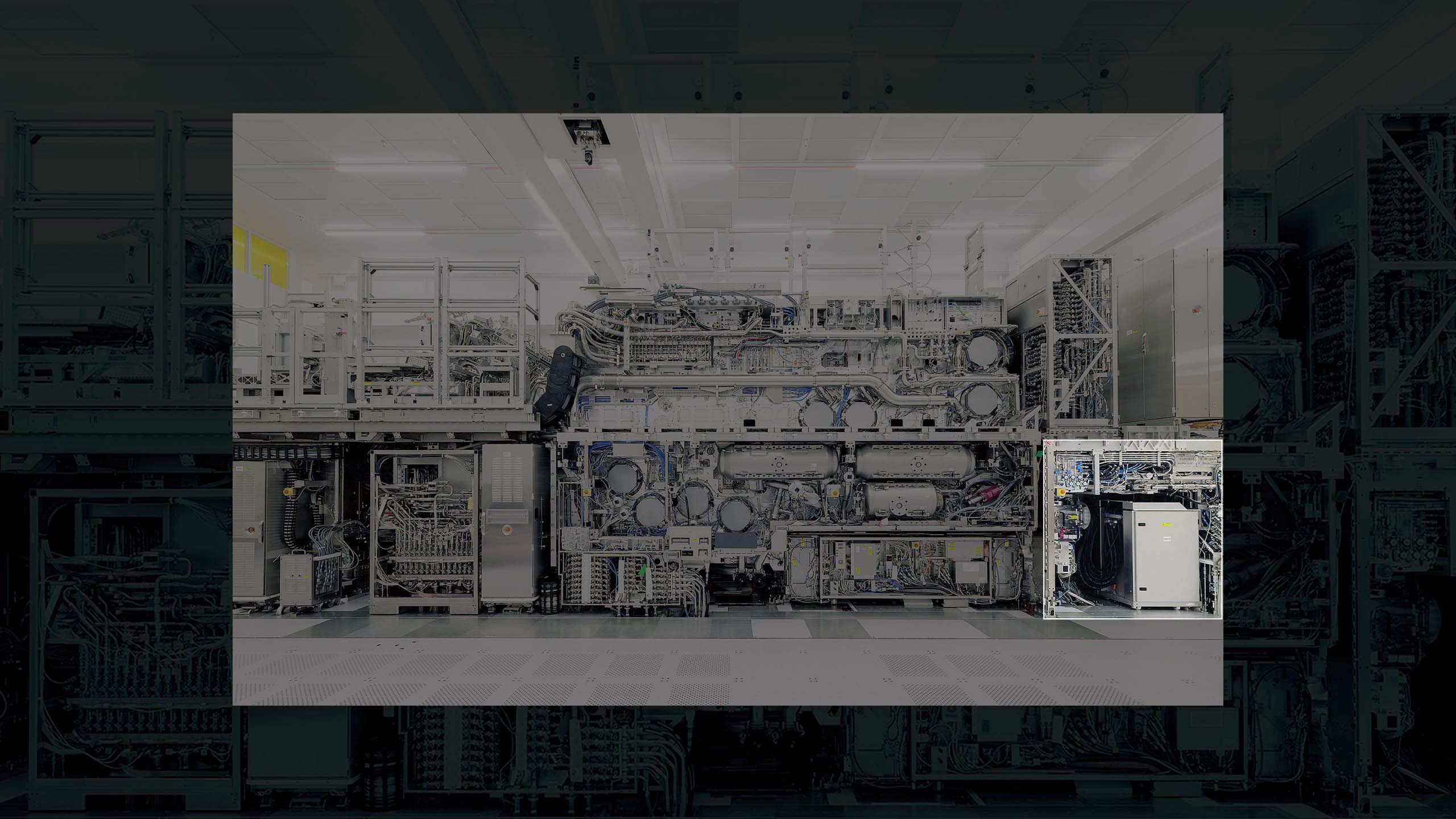
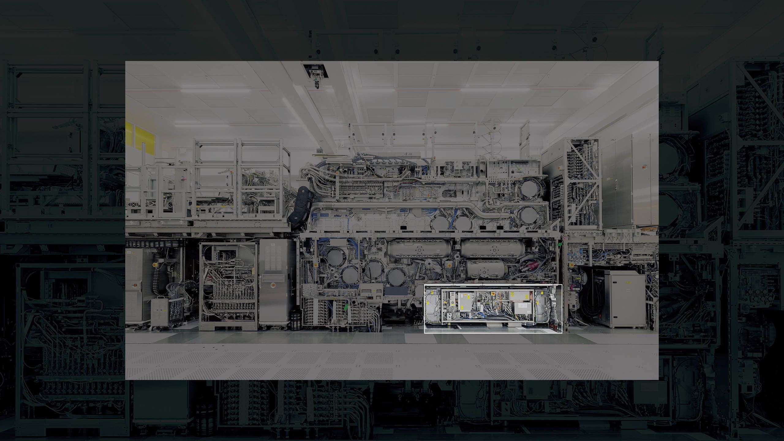
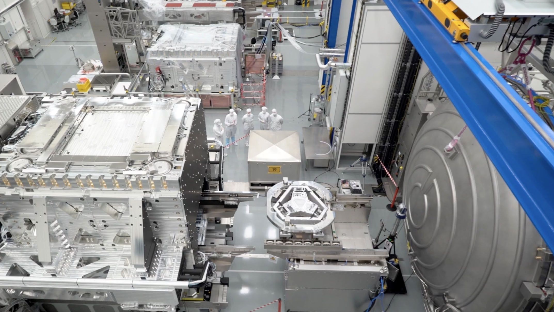
At the cutting edge of chips
ASML's high-NA EUV lithography machine weighs 150,000 kg, stretches 14 meters long by 4 meters high and 4 meters wide, and is made up of millions of components. Industry sources call it the most complex machine ever built.
(Photo courtesy of ASML)
(Video courtesy of ASML)
(Video courtesy of ASML)
In the source vessel, EUV light is generated by a powerful laser striking 50,000 tiny droplets of tin per second. This light is used to print the chip features on the wafer.
——
Key suppliers: Trumpf (laser), Cymer (EUV light source)
(Video courtesy of ASML)
(Video courtesy of ASML)
The reticle handler holds the mask, or reticle, that contains the pattern to be printed on the wafer. The reticle moves with extreme acceleration, and this speed is key to producing more chips per hour.
——
Key supplier: ASML's team in Connecticut
(Video courtesy of ASML)
(Video courtesy of ASML)
In the wafer handler, precision robotic arms transfer wafers in and out of the system's vacuum environment, operating with high positioning accuracy and at a consistent temperature.
——
Key supplier: VDL
(Video courtesy of ASML)
(Video courtesy of ASML)
The wafer stage positions the wafer with a precision of less than a nanometer -- about 4 silicon atoms -- for each exposure, checking and adjusting 20,000 times per second.
——
Key supplier: VDL
(Video courtesy of ASML)
(Video courtesy of ASML)
The illuminator, working with the projection optics, collects and shapes the EUV light in a high vacuum environment, because EUV is absorbed by everything -- even air. The projection mirror is the smoothest surface ever made by humans.
——
Key supplier: Carl Zeiss
Jos Benschop, ASML's executive vice president of technology, described the development of EUV machines as the company's toughest challenge.
EUV machines had to be completely redesigned, as its light source has a wavelength of just 13.5 nanometers, compared to 193-nanometers used in earlier DUV systems. In general, the shorter the light wavelength, the finer the chip design circuit patterns that can be printed.
It took more than 20 years to turn the EUV concept into a commercial reality. While the first sample machines were shipped to clients in 2006, it wasn't until 2019 that TSMC and Samsung were using them to produce the world's most advanced chips.
Developing high-NA EUV, the next generation of the technology, was just as complex. It took more than eight years, for example, just to redesign the projection optics and illumination systems, the core part of the machine that shapes and focuses the light to project chip designs onto wafers.
The NA in the machine's name stands for numerical aperture, a measure of the ability of an optical system to collect and focus light. NA is a key factor in determining how finely circuits can be printed onto wafers. In simple terms, a higher NA means a machine can print smaller chip features.
ASML supplier Carl Zeiss says the optical system in a high-NA EUV machine contains around 65,000 parts and takes a year to produce. Developing the system took over 10 million working hours and 25 years of collaboration with ASML, the company told Nikkei Asia.
The sheer complexity of these machines is one of ASML’s greatest competitive advantages.
Chiang Shang-yi, a board director of Foxconn and former R&D chief of TSMC, described lithography as “the most complex and resource-intensive step in chipmaking” and lithography machines as harder to build than other chip equipment.
“ASML’s exclusivity, particularly in EUV tools, is greater than that of TSMC, the world’s top chipmaker, in making cutting-edge chips. Its success comes not only from developing its own technology but also from exclusive partnerships with top suppliers like Zeiss and Cymer.”
ASML acquired Cymer in 2013 and took a nearly 25% stake in Carl Zeiss SMT, a subsidiary of Zeiss making advanced optics, in 2016.

Zeiss of Germany is ASML's exclusive partner in making advanced optical systems. (Photo courtesy of Zeiss)
Zeiss of Germany is ASML's exclusive partner in making advanced optical systems. (Photo courtesy of Zeiss)
The company itself acknowledges that its lithography empire rests not only on its own know-how but on the support of thousands of suppliers.
"This is a huge amount of competence, and different people work on different parts of the tool," ASML's CEO Christophe Fouquet, told Nikkei Asia. "Most of the time the people, for example, who worked on the light source don't know at all how the optic [system] is working, because these are very different domains of competence."
Fouquet described the development as "basically bringing together a huge amount of knowledge. ... It's extremely difficult for anyone to be able to reproduce an EUV in just a few years."
Andreas Erdmann, head of computational lithography and optics at top German research center Fraunhofer IISB, said this complexity is a hurdle for would-be challengers. "If you are building lithography machines, it's not only good optics you need," he told Nikkei Asia. "You will need mechanics, electronics, chemistry, mathematics and computation. Everything has to work together and integrate perfectly. That's why so few players can do that in the world."
There being "so few players," as Erdmann puts it, is something of a mixed blessing for the Dutch company.
As the primary player in a critical field, it has been caught in the crossfire of the U.S.-China tech rivalry. Washington has imposed increasingly strict export controls aimed at restricting ASML from shipping advanced tools to China and has pressured the Dutch government to issue similar rules. The latest U.S. regulations bar ASML from exporting any immersion DUV machines or more advanced systems to China without a license.
Its U.S.-listed shares are down over 20% over the past year amid macroeconomic headwinds and geopolitical uncertainties.
"ASML often felt it was particularly targeted by the U.S. because of its outstanding market position," a Dutch diplomat familiar with the U.S.-Netherlands talks on export control rules told Nikkei Asia.
What would have been China's first EUV machine shipment -- from ASML to SMIC in 2019 -- was blocked due to U.S. pressure, Nikkei Asia first reported. A former U.S. Commerce Department official said export controls, especially on access to cutting-edge lithography tools, have been effective in slowing China's progress in advanced chip manufacturing.

Huawei has stepped in as a key supporter of China’s chipmaking equipment sector. (Photo by Cheng Ting-Fang)
Huawei has stepped in as a key supporter of China’s chipmaking equipment sector. (Photo by Cheng Ting-Fang)
"To build cutting-edge chips at scale, you simply need EUV machines," the former official said.
These political tensions have turned China, a key market, into one of ASML's most determined competitors, even if the road to success turns out to be a long one.
China's Shanghai Micro Electronics Equipment (SMEE), for example, was set up 23 years ago and has developed lithography tools capable of producing 90-nm chips, suitable for use in home appliances, some consumer electronics and cars that require less computing power. The company aims to introduce lithography systems for 65-nm and 28-nm-grade production, but adoption of its machines by Chinese chipmaking clients remains limited.
"I visited a chipmaking client and saw SMEE's lithography machine and I asked how it was," an executive with a Chinese chip equipment maker said. "My client told me it's been in place in the facility for a year but still doesn't work properly."
And this for tech that is far less advanced than EUV lithography machines.
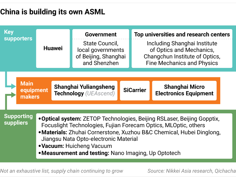
Huawei, itself long subject to U.S. blacklisting, has stepped in as a key supporter of China's chipmaking equipment sector.
The company has built a massive R&D hub in Shanghai, and is recruiting talent from global chip leaders like TSMC, ASML, Applied Materials and KLA. It is also supporting SiCarrier, a Shenzhen-based chip tool maker founded in 2021, in the development of a wide range of chipmaking tools, aiming to lower dependence on foreign players. Huawei has also hired optics and simulation experts overseas for its research institutes in Germany, a source familiar with the matter said.

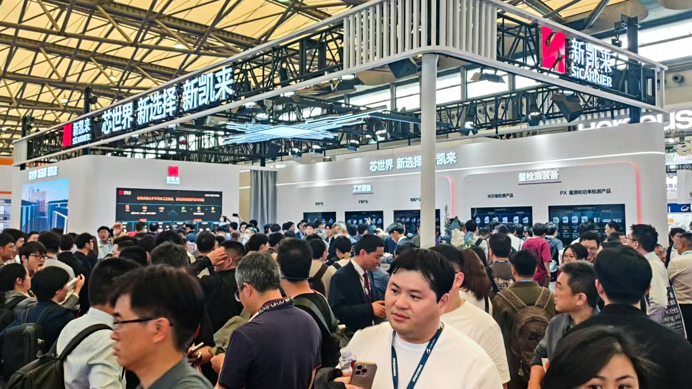
Huawei-linked chip equipment maker SiCarrier made its debut at the Semicon China 2025 industry trade show.
Huawei-linked chip equipment maker SiCarrier made its debut at the Semicon China 2025 industry trade show.
Little-known Shanghai Yuliangsheng Technology, meanwhile, has emerged as a lithography challenger thanks to support from Huawei and SiCarrier, Nikkei Asia has learned. The company, also known as UEAscend, is also receiving technical help and staff from SMEE and several top research institutes, sources said.
Huawei, SiCarrier and Yuliangsheng are working together to develop China's first immersion DUV lithography machines in hopes of rivaling global leaders like ASML and Nikon, two people with knowledge of the matter said.
The trio's ultimate mission is to develop a homegrown EUV lithography machine and build an independent ecosystem free from U.S. restrictions, they said. The central and local governments are also throwing their weight behind such efforts.
Huawei, SMIC, YMTC, CXMT, SMEE and SiCarrier did not respond to requests for comment.


The sense of urgency is growing. SMIC, for example, still relies on foreign tools it acquired before export controls to produce advanced chips, such as those at the 7-nm grade, for Huawei and other Chinese chip developers. A breakthrough in lithography and other equipment would help China gradually increase its output of these state-of-the-art chips.
To support this push, China launched the third phase of its National Integrated Circuit Industry Investment Fund -- known as the Big Fund -- in May 2024, with 344 billion yuan ($48 billion) in government backing. This phase focuses on strengthening the lithography supply chain and is expected to attract 1.38 trillion yuan in private investment, according to government data. Local governments from Beijing to Shanghai and Shenzhen have also introduced policies to back domestic suppliers of critical EUV components, including photoresists, lithography tools, mirrors, lenses, lasers and light sources.

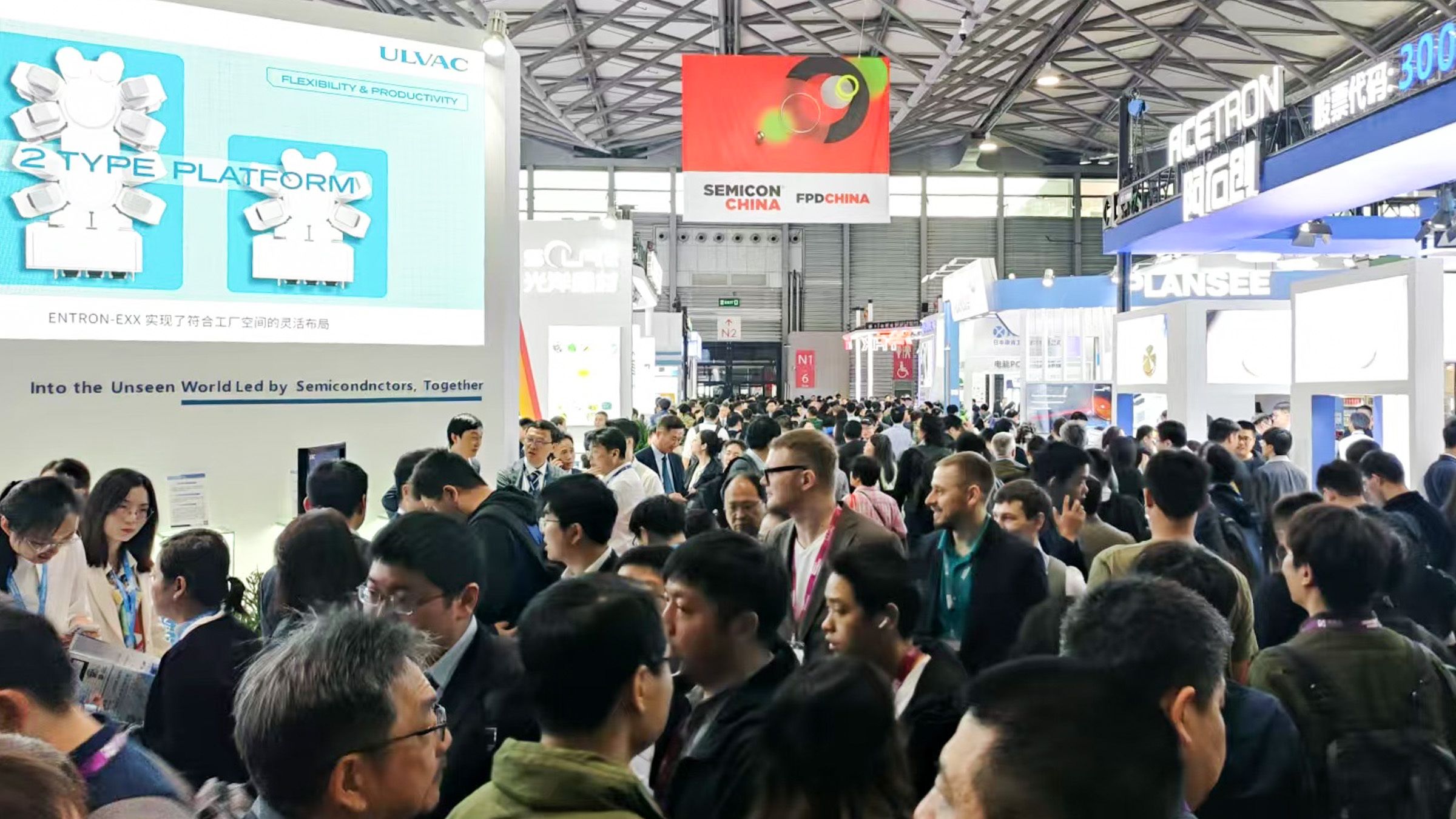
Local chip industry fairs have become a great opportunity for China's chip toolmakers to expand their business.
Local chip industry fairs have become a great opportunity for China's chip toolmakers to expand their business.
Lithography expert Lin Burn-Jeng, a former senior TSMC executive and current dean of the College of Semiconductor Research at National Tsing Hua University in Taiwan, said becoming competitive in lithography requires more than money.
"You need support from chipmakers, along with accumulated experience and technology. In particular, building competitive lithography machines demands extraordinary precision engineering, down to just a few nanometers," Lin said.
Mitsunobu Koshiba, former chairman of Japanese photoresist maker JSR, described ASML's machines as the "most complicated tool on this planet" and not something that every country can hope to produce.
Motivation is another key ingredient to success, one that, ironically, Washington has provided. U.S. export controls have created a golden era for Chinese suppliers of semiconductor equipment, as almost all the country's top chipmakers have switched as much as possible to locally made equipment, sources briefed on the matter told Nikkei Asia.
"To be honest, most domestically built equipment still can't match the performance of leading international solutions," said one Chinese chip equipment executive. "But at this stage, chipmakers have no choice. They need to use them as a baseline and keep giving them a chance, even if it means risking impacts on production quality."

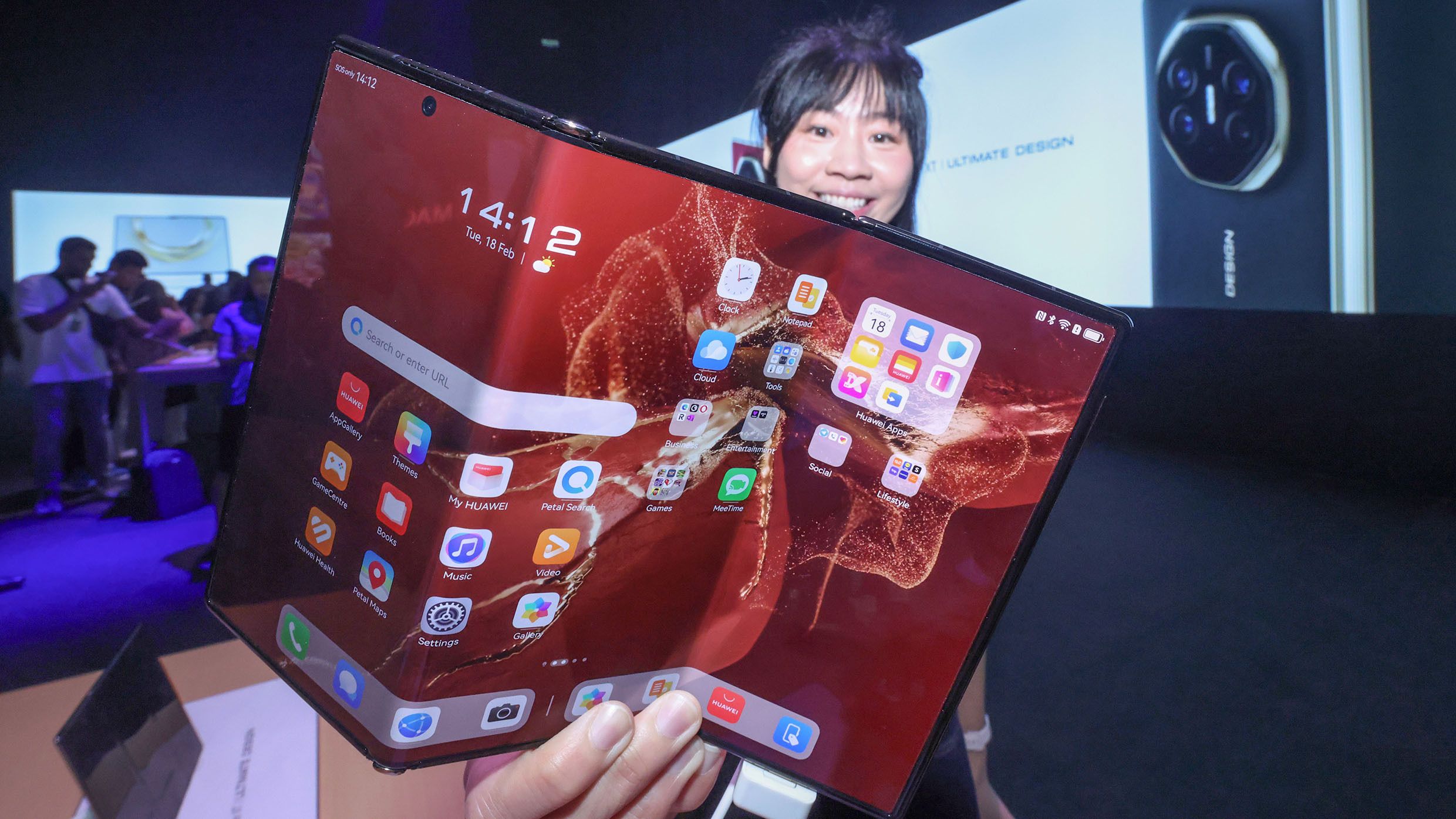
Huawei unveils its Mate XT trifold smartphone at an event in Malaysia on Feb. 18. (Photo by Yuki Kohara)
Huawei unveils its Mate XT trifold smartphone at an event in Malaysia on Feb. 18. (Photo by Yuki Kohara)
Both SMIC and CXMT, the country’s top DRAM memory chipmaker, have experienced significant yield loss due to the use of domestic equipment, something global chipmakers typically try to avoid, Nikkei Asia has learned. However, this has not stopped them from continuing their trials, according to several supply chain executives familiar with the matter.
Chinese chipmakers are also continuing to stockpile equipment from global leaders when possible, purchasing nearly $34 billion worth of such tools from Japan between 2020 and 2024, according to Nikkei Asia analysis of Chinese customs data.
"Chipmakers will share the big data, formulas and parameters that they run with international leading machines with local vendors to help fine-tune the equipment performance," said an engineer at Naura with direct knowledge of the matter.
In many cases, Chinese companies buy foreign chip equipment not for production but to research how subsystems and components are put together, according to multiple industry executives. "This is the so-called reverse engineering," one of the industry executives said.
U.S. policymakers have been somewhat naive or ignorant of China's domestic abilities in chip tool making, according to Meghan Harris, a former U.S. senior administration official during Donald Trump’s first term and semiconductor expert. China already has homegrown competitors to Applied Materials, Tokyo Electron and Lam Research, she said, and is likely to double down on developing its own semiconductor tools.


"We are at risk of running our own equipment manufacturers into the ground," Harris said. "The worst-case scenario is that Chinese toolmakers become not only domestically competitive [but] even internationally competitive, which is coming ... Once that starts, it will be very difficult to stop."
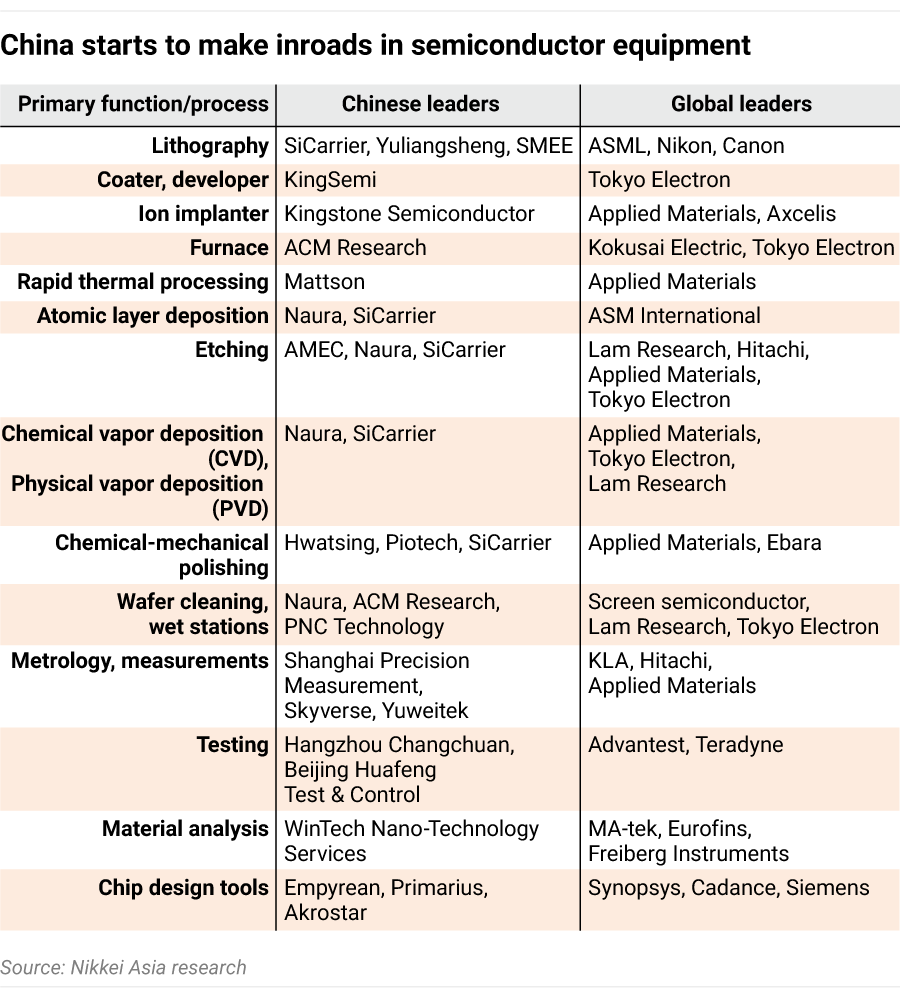
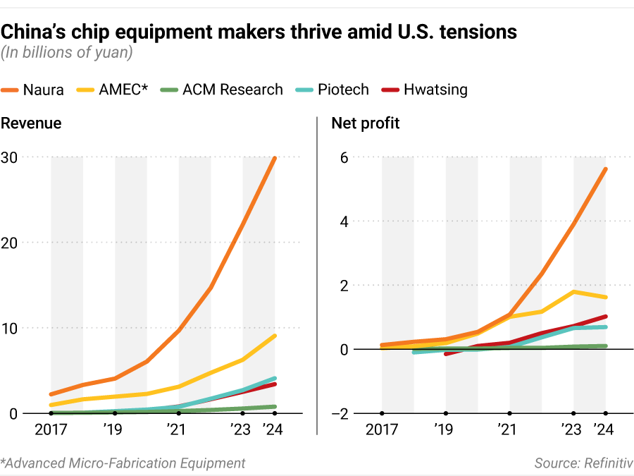
Indeed, China's top five chip tool makers have flourished amid the escalation of U.S.-China tensions since 2019. Their combined revenue has grown by 473% since 2019, with four out of five reporting record profits in 2024, Nikkei Asia's analysis found. In every chipmaking step except lithography, China now has its own player that could potentially challenge global leaders. Naura, often referred to as China's version of Applied Materials, is now the world's sixth-largest chip tool maker by revenue.

In lithography, China's short-term strategy remains stockpiling. To hedge against further export controls, China purchased 8.92 billion euros ($10.45 billion) worth of tools from ASML in 2024. That rush of orders led to China accounting for 41% of ASML's system sales that year, the highest share of any market, though the company expects that figure to drop to around 20% this year amid export restrictions.
But the incentive to replace the Dutch leader remains strong.
"China has made tremendous progress in nearly every category of semiconductor equipment but lithography," Charles Shi, a semiconductor analyst at U.S. investment bank Needham, told Nikkei Asia. "China is clearly trying to develop their own lithography technology. It will take time, but the huge stockpile of ASML tools inside China has clearly bought them time."

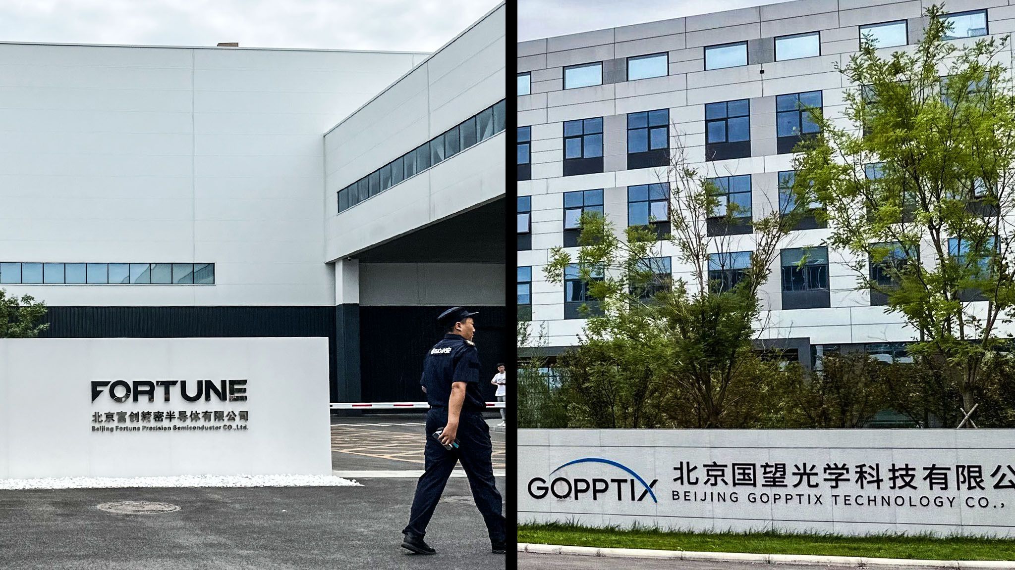
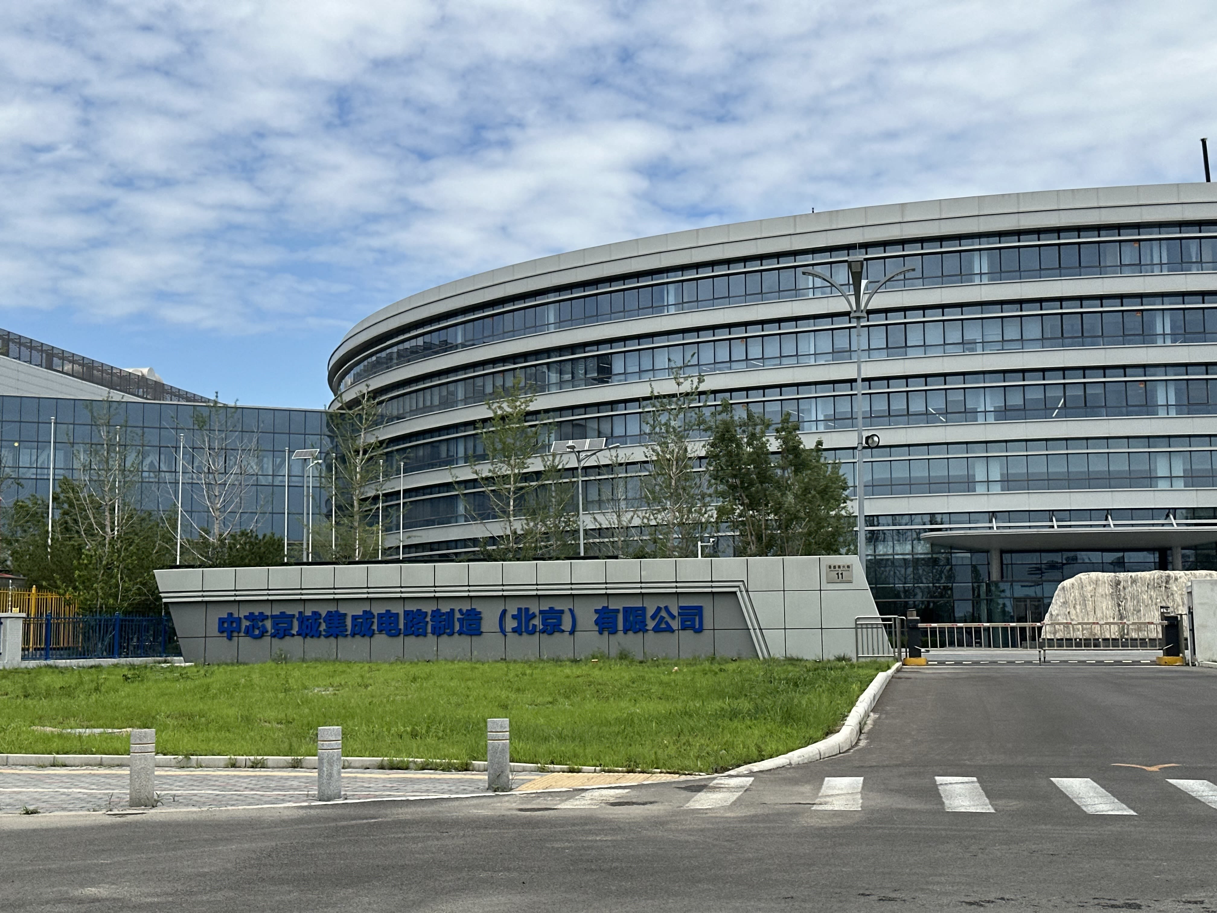
Gopptix and Fortune Precision, key local chip equipment component suppliers, are expanding plants next to SMIC's facilities in Beijing.
Gopptix and Fortune Precision, key local chip equipment component suppliers, are expanding plants next to SMIC's facilities in Beijing.
In its most recent annual report, ASML acknowledged that it faces competition from new players with substantial financial resources, as well as from competitors driven by geopolitical factors to become self-sufficient.
China's opportunity also lies in the slowdown of Moore's Law, as squeezing more transistors into a smaller area has become increasingly difficult and costly. While advances in lithography remain essential, advanced chip packaging has emerged as an alternative approach for boosting chip power by integrating multiple chip components together.
With lithography no longer the only route to improving computing power and only a handful of top global chipmakers able to afford ultra-advanced tools like high-NA EUV systems, rising competition from China would pose serious challenges for the current chip tool leaders.
"The whole industry is closely monitoring the rising Chinese competition. Right now, they're buying more than they need from us, but we know they are aggressively trying to replace us," said an executive with a Japanese chip tool supplier. "If they make breakthroughs, it will create a huge pressure on [non-Chinese] suppliers."
The barriers to entry are much higher for lithography than for other types of chip machines, according to Didier Scemama, head of EMEA IT hardware research at BofA Global Research. But given that DUV and EUV technologies have already been around for many years, he expects China to eventually make some progress.
"It could be in five years, it could be in 10 years, it could be in 15 years. We don't really know," Scemama said. "Is that going to be competitive with what ASML does? [That is] highly unlikely. But it's good enough for China."